KubiSat hardware: building a 1U CubeSat model from discrete components
A walkthrough of the electronics inside KubiSat - a 1U CubeSat model designed for a stratospheric balloon flight. Three PCBs, lithium-ion power with MPPT solar charging, an RP2040 controller, LoRa radio, GPS, RTC, SD storage and a small sensor array.
KubiSat is a 1U CubeSat-format model built to fly on a stratospheric balloon. Picking the components was not trivial: the model has to keep working in a wider temperature range than typical consumer electronics, and the GPS receiver has to keep producing a fix up to roughly 50,000 m above sea level. Higher altitude also means lower temperature, which drops the capacity and efficiency of the battery and forces a more careful power design and a thermally insulating enclosure.
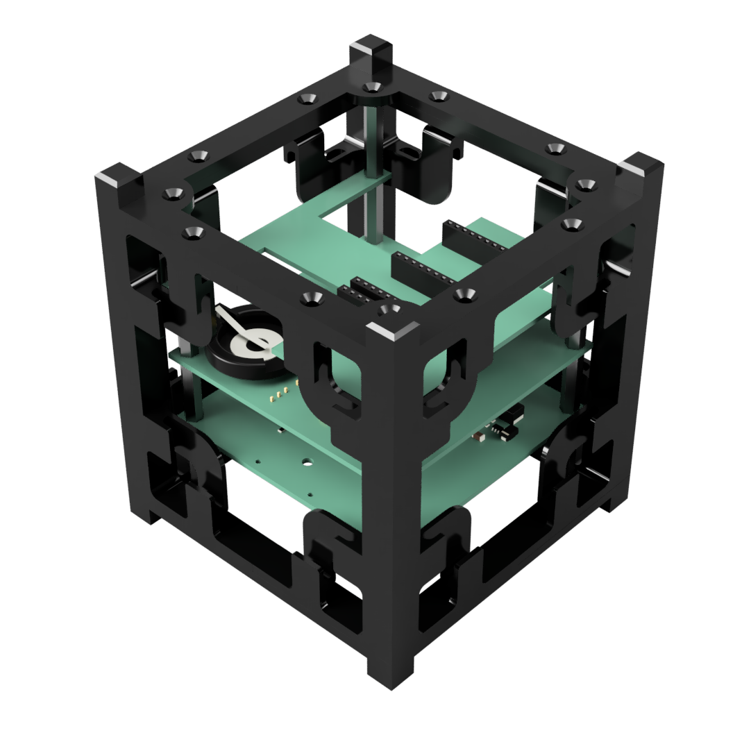
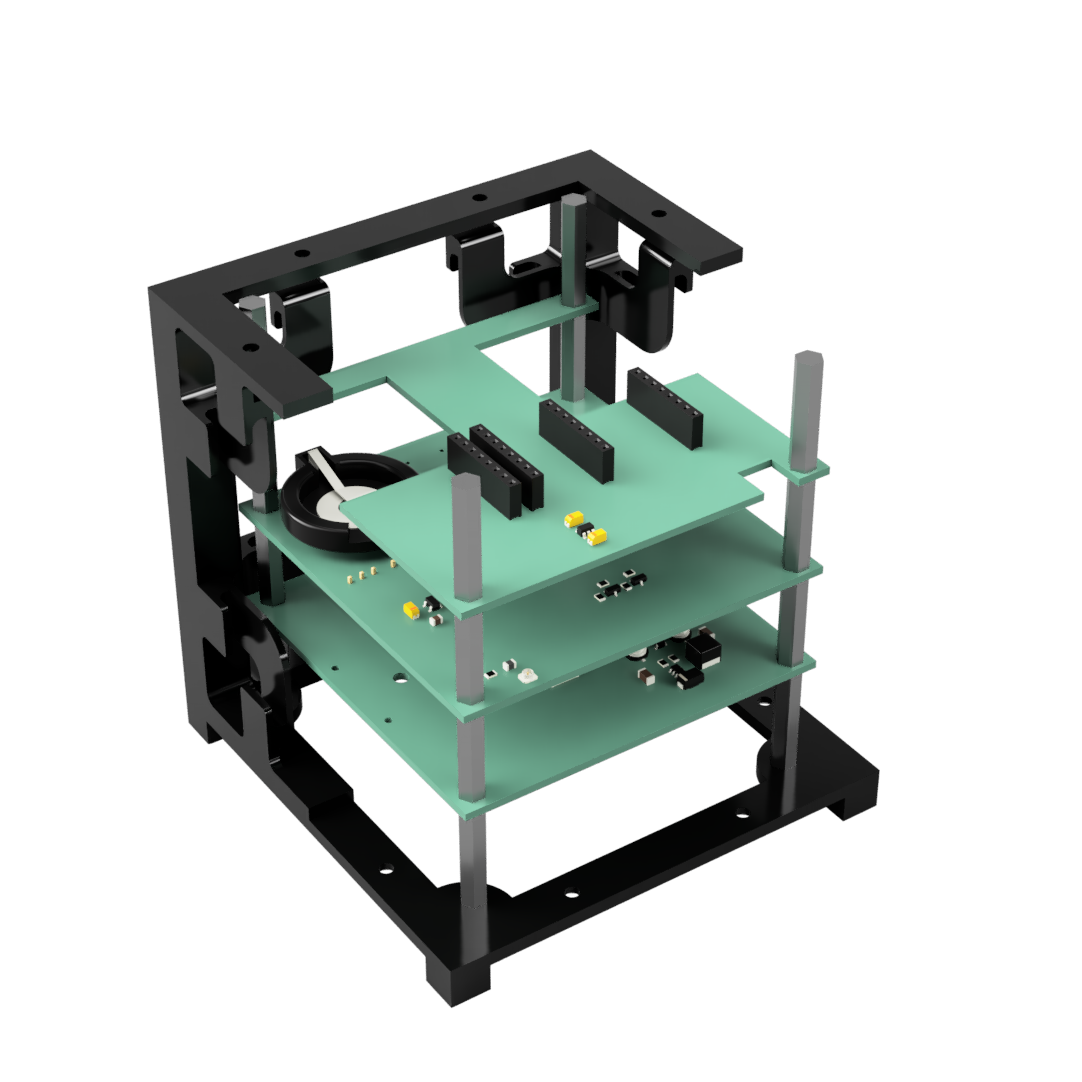
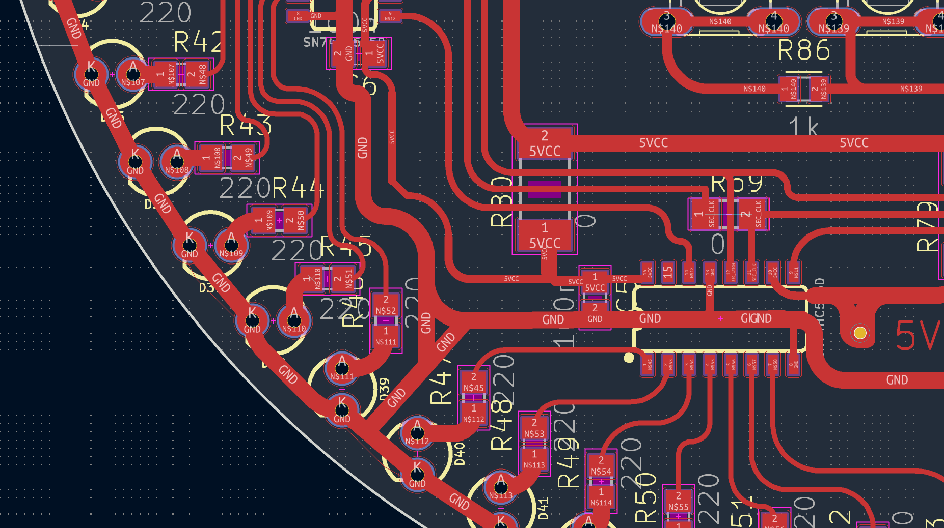
The hardware is split into three independent PCBs: a power board, a main controller board and a sensor board. Each board has its own connector and can be developed and tested on its own.
Power module
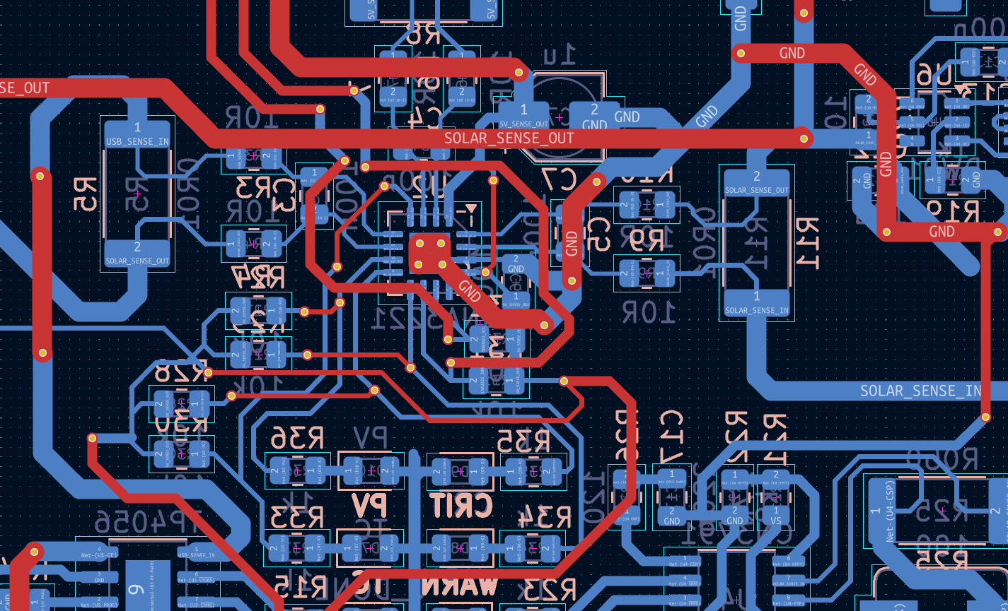
The power board carries the battery pack, the battery protection circuit, two chargers, a 5 V buck converter and a current/voltage monitor. The board exposes a single 6-pin JST connector with I2C, the 5 V rail and two ground pins.
Energy storage is two 18650 lithium-ion cells, 3.7 V nominal, 2000 mAh each. Wired in series they give 4000 mAh of capacity at a nominal pack voltage. At a typical system draw of about 40 mA the theoretical run time is around 100 hours, but in practice it is shorter because of the GPS, the radio and converter losses. With the GPS in high-performance mode (about 80 mA) the total current is around 120 mA, which still gives roughly 33 hours of runtime - well above the ~3 h that a balloon flight typically takes.
Because the model is recovered after the flight, the power system is designed to be recharged on the ground over USB-C. Four solar panels are mounted on the side faces of the enclosure for the charging experiment in flight - because the base is square, only two panels can be at peak illumination at any time.
INA3221 current and voltage monitor
All voltages and currents are measured by an INA3221 over I2C. The chip is powered from 5 V, so a level shifter is needed to talk to the 3.3 V RP2040. INA3221 has a stated accuracy of about 0.5% and a quiescent current of around 1 mA in continuous mode.
The three channels are used as:
| Channel | Use |
|---|---|
| 1 | Battery voltage and USB charging current |
| 2 | 5 V rail voltage |
| 3 | Solar charging current |
Sample averaging is configurable from 1 to 1024 samples. I use 16-sample averaging in continuous mode as a balance between noise and update rate.
Battery protection (DW01A + FS8205A)
Cell protection is done by a DW01A plus an FS8205A dual N-channel MOSFET. The DW01A limits the cells to a window between 2.4 V and 4.3 V, both for over-discharge and over-charge. The FS8205A is wired as a bidirectional switch (two N-FETs source-to-source), so a single component can cut both charge and discharge paths without extra diodes. Quiescent current of the DW01A is about 3 µA, which is negligible compared to the self-discharge of the cells.
USB charger (TP4056)
USB-C charging is done by the very common TP4056 in CC/CV mode. The CC1/CC2 pins are configured for a fixed 5 V supply. Charging current is configurable up to about 1 A; I set it to ~780 mA to keep the chip from overheating in the closed enclosure. Efficiency is around 80%, which is typical for a linear lithium charger.
Solar charger (CN3791)
The solar panels feed a CN3791 MPPT buck charger. It takes 4.5-28 V on the input and can hit up to 96% efficiency. The MPPT operating point is set to 4.9 V, which matches the panels I use:
| Parameter | Value |
|---|---|
| Nominal voltage | 5.5 V |
| Nominal current | 110 mA |
| Peak power | 0.55 W |
The four panels are wired in series to lift the voltage.
5 V buck converter (LN2220)
The pack voltage is stepped to a regulated 5 V rail by an LN2220 synchronous buck. At a typical 120 mA load it sits around 90% efficiency. Switching at 1.2 MHz lets the passives stay small, which matters in a 1U enclosure. The rail is regulated to 5 V ±2% with built-in short-circuit, over-temperature and under-voltage protection.
Main controller board
The main board carries a Raspberry Pi Pico, a LoRa SX1278 radio, a NEO-6M GPS module, a DS3231 RTC and an SD card slot. The board breaks out separate connectors with I2C, SPI and a 5 V supply for the sensor board.
RP2040
The MCU is a dual-core ARM Cortex-M0+ RP2040 clocked at 133 MHz with 264 kB of SRAM and dual UART, SPI and I2C peripherals. I picked it for the availability, price, the official SDK and the size of the community around it. The firmware lives in QSPI flash next to configurations, logs and measurement files. The 3.3 V the chip needs is generated by the Pico board itself from the 5 V rail.
LoRa radio (SX1278)
The radio is a 433 MHz SX1278 LoRa module running half-duplex at up to 300 kbps. Output power is +18 dBm, which is enough for line-of-sight communication of several hundred meters in normal conditions and is documented to work over 700 km in optimal cases. It talks SPI to the RP2040 at 8 MHz on its own dedicated SPI bus.
Current draw at 433 MHz is:
| State | Current [mA] |
|---|---|
| Receive | 12.1 |
| Transmit | 93 |
| Standby | 1.6 |
GPS receiver (NEO-6M)
The GPS module is a NEO-6M on the L1 band (1575.42 MHz) feeding NMEA-0183 over UART once per second. Position accuracy is around 2.5 m, which is enough to recover the model after landing. Because finding the model is more important than saving energy, the GPS is always powered on in flight mode and cannot be turned off remotely.
GPS power is gated by a small DC-DC converter with an EN pin tied to a GPIO. A cold start takes about 30 s while the receiver downloads the full ephemeris. A CR2032 backup cell keeps the almanac and the last fix between sessions, which drops the time-to-first-fix on a warm start to 1-3 s.
Real-time clock (DS3231)
The RTC is a DS3231 with a built-in temperature-compensated crystal oscillator and a thermometer, talking I2C. Accuracy is ±3.5 ppm between -40 °C and +85 °C, which is at most about 9 seconds per month of drift. The chip handles months and leap years on its own. The same CR2032 backup cell that holds the GPS data also keeps the clock running across power cycles, which matters because every measurement is timestamped.
Storage (SD card)
Logs, telemetry and event data are stored on a 2 GB SD card mounted on its own SPI bus, so other peripherals do not contend with it. The card holds two kinds of data: full telemetry records (sensor readings, voltages, currents, GPS position, date and time) and event logs (under-voltage events, clock changes, etc.) with full timestamps. The contents can also be read out remotely over the radio.
Sensor board
The sensor board is intentionally simple - it exposes 5 V, an I2C bus and an SPI bus through four 8-pin headers on a 2.54 mm pitch, so up to four sensors can be plugged in at once.
BME280 - pressure, temperature, humidity
The BME280 is a Bosch combo sensor (pressure, temperature, humidity) in a 2.5 × 2.5 × 0.93 mm package. I wired it on I2C for simpler routing. It gives:
- 300-1100 hPa pressure with ±1 hPa accuracy
- -40 to +85 °C temperature with ±1 °C accuracy
- 0-100 %RH humidity with ±3 % accuracy
Current draw is around 3.6 µA at 1 Hz. The pressure reading is useful for an independent altitude estimate, since 1 hPa is about 8.3 m of height at low altitudes.
BH1750 - light
The BH1750 is a 16-bit digital lux meter with a spectral response close to the human eye. It covers 1-65535 lx, with selectable 0.5/1/4 lx resolution. Active current is 120 µA and sleep is below 1 µA. Apart from logging ambient light, sharp changes are useful as a marker (sunlight vs. shadow) when looking at temperature data later.
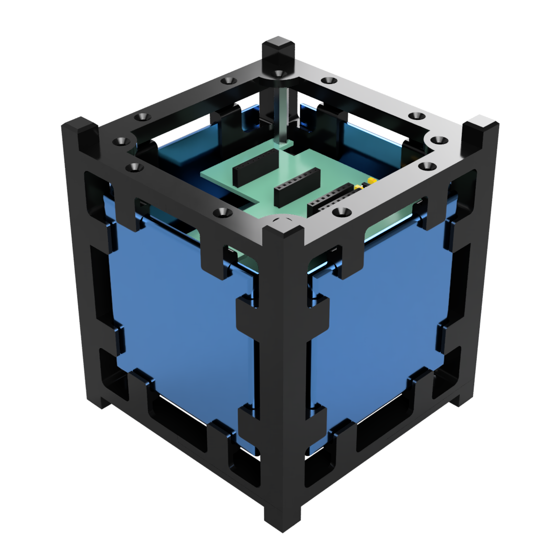
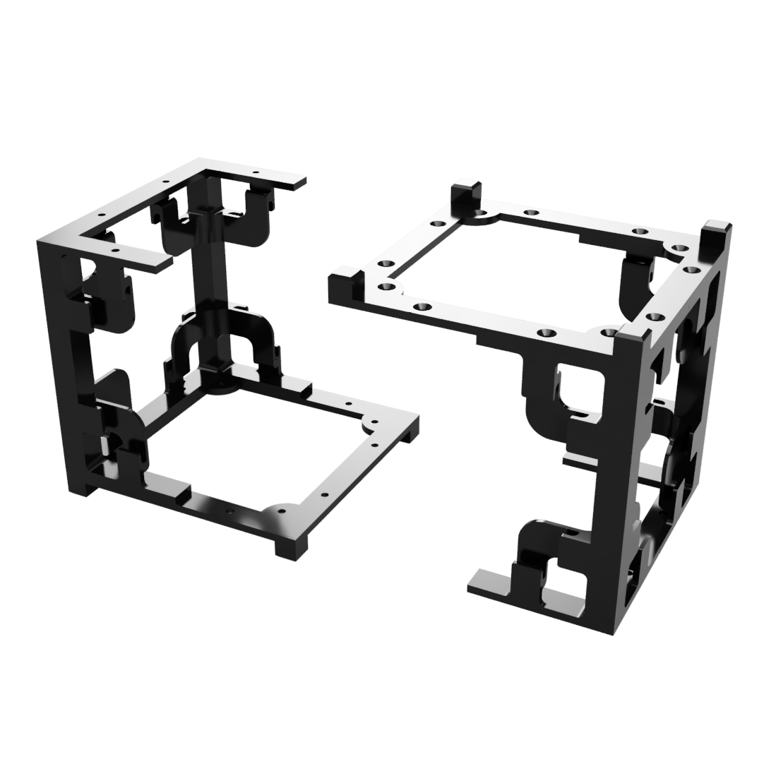
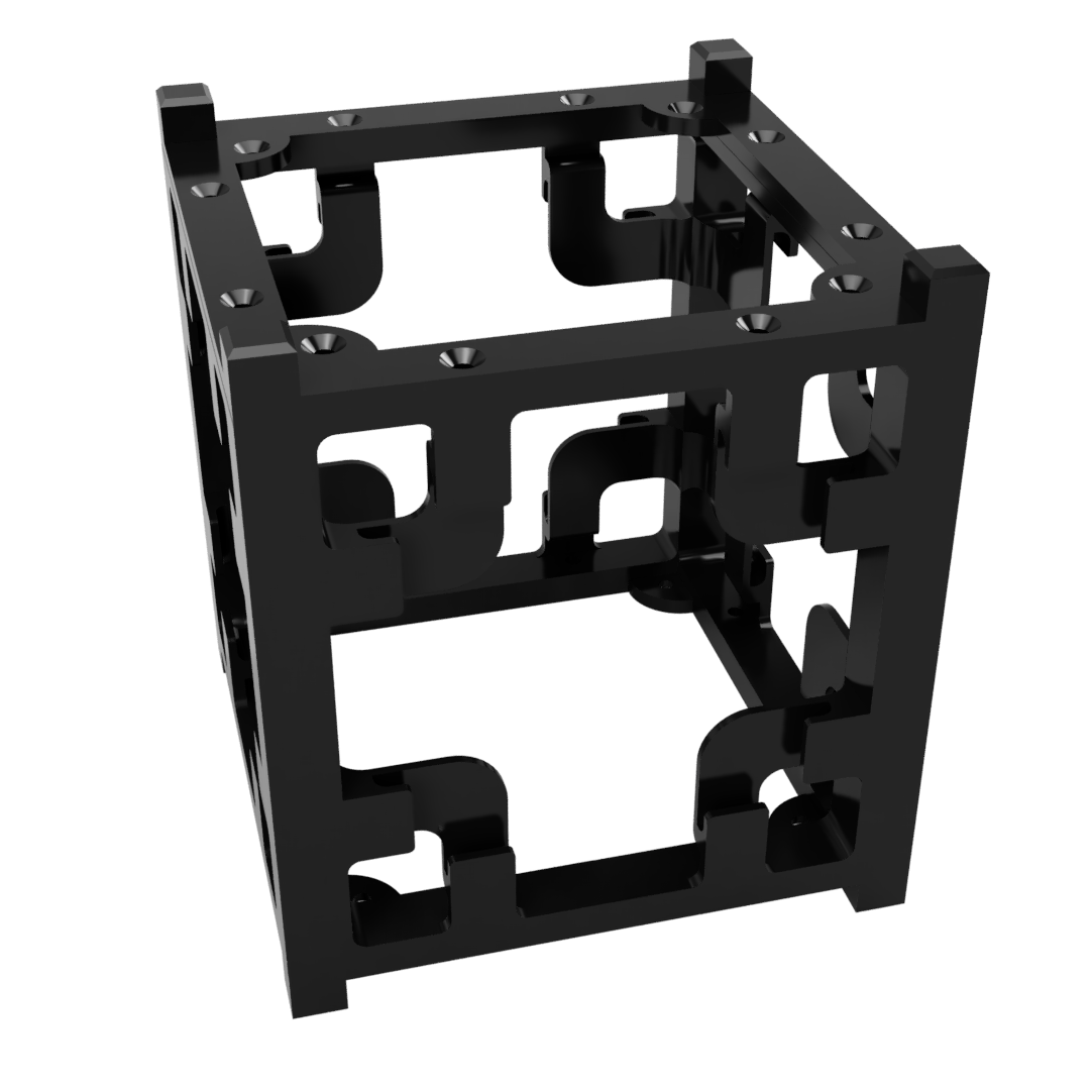
Enclosure
The case was designed in Autodesk Fusion 360 and follows the CubeSat 1U spec - 100 × 100 × 113.5 mm. It is split into six parts: four corner pieces and two base plates, all printable on a standard FDM machine. The base plates are 10 mm thick, which is a trade-off between rigidity and internal volume. Mounting holes are 3 mm diameter for both the corner-to-base joints and the PCB stand-offs.
Each PCB is mounted on 22 mm polyamide stand-offs so that the total stack height of the boards plus the spacers equals 93.5 mm, which prevents mechanical stress on the housing. The enclosure splits into two halves to give full access to the inside; the inner volume is wide enough to reach the batteries and the USB connector from the bottom, and the sensors and connectors from the top.
The four side faces each carry a 70 × 70 × 3 mm solar panel mount. Because of the square footprint at most two panels can produce full power simultaneously, which is the constraint that defines the upper bound of the in-flight charging experiment.
What I would change
The biggest single improvement would be the solar charging configuration. The current four-panel layout works, but switching to more, smaller cells wired so that the input voltage to the CN3791 is consistently higher would improve charging efficiency significantly. The rest of the architecture - three separate PCBs, well-isolated buses, full current/voltage monitoring on the main rails, and an MCU with two cores - has held up well across development.